
Why testability?
Design for Testability (DFT)
is just one aspect of the current clamor about a variety of initiatives
aimed at speeding innovative, high quality, customer-driven new
products to market in a timely, profitable manner. Whatever the
name -- concurrent engineering, continuous improvement or quality
function deployment -- these technology buzzwords often deliver
more in rhetoric than in reality.
Encompassing such grand concepts as design for manufacture, design for testability, design for use, design for quality, and design for service, they tend to fall short of their goal. The primary reasons are that managers, supervisors, and engineers fail to understand the total cross-functional commitment needed for success, and are not fully aware of the tools and techniques needed to implement these programs.
 |
any manufacturing process |
What is testability?
Testability can best be described
as the ease with which the functionality of any electronic product
circuit or component can be determined to a desired degree of
accuracy. To put it more simply, how easily can it be checked
for performance to-spec throughout the entire product life cycle
from product concept through design, manufacture, and service?
How quickly can test programs be generated? How accessible are
the test points? How comprehensive is the fault coverage?
Testability is not a technological
innovation. It is a mindset that creates a constant awareness
of the importance of ease-of-testing ... in engineering ... during
production ... in the field. Testability is critical to the manufacturing
process -- a product that cannot be readily tested is not really
manufacturable.
Non-testability costs;
testability pays.
Unpredictable production schedules,
bonepiles of suspect boards, a very high cost of test, and an
uncertain level of product quality delivered to the customer...
these are the indirect costs of non-testability. Add the time
spent trying to diagnose, and you quickly see that non-testability
can be very expensive.
Testability, on the other
hand, is introduced at the design stage, where it dramatically
lowers the cost of test and the time spent at test. Properly managed,
testability heightens your assurance of product quality and smoothes
production scheduling.
What are the benefits of
testability?
The time and money saved by
designing for testability are the obvious major advantages -- the
more efficiently and accurately you test the more profitable the
product But there are many others.
Designing for testability:
GenRad's Commitment to
Design for Testability.
As the recognized test technology
leader, GenRad offers a full spectrum of DFT products, services
and consultancy to electronic manufacturers. All of our products,
experience, test knowledge and engineers are dedicated to facilitating
design for testability. Our goal is to help you speed new designs
into production at lower overall cost while, simultaneously, assuring
high levels of product quality and product profitability. In
short, to make you more competitive.
Testability Challenges...
the Management Issue.
Because DFT is essentially
a management issue and not a technology issue, any testability
effort must have management's full commitment and support if it
is to succeed. Management needs to be aware of the enormous opportunities
for savings as well as the technology, tools, and products available
to support testability, all the way from design right down to
the manufacturing floor. Before the advantages of the potential
economic benefits of a well integrated DFT program can be realized,
it is critical that the state of testability technology be well
understood.
Each major advance in technology
signals a new set of design, manufacturing, and testing challenges
to be overcome. Each successive generation of test engineer has developed
new test techniques as device, packaging, and interconnect technologies
have evolved from point-to-point wiring to through-hole printed
circuit boards and to surface mount technology.
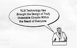 |
VLSI technology has put
the design of truly untestable circuits within everyone's reach.
SMT and VLSI technology
have teamed up to produce extremely complex circuit designs, with
data rates approaching 100 MHz becoming commonplace; device miniaturization
that a Lilliputian would dwarf, and a significant
decrease in electrical test access. These add up to a serious
threat to the foundations of in-circuit test.
The emergence of multi-chip
modules, direct chip attach, and optical coupling technologies
will simply hasten the pace at which testability must be re-invented.
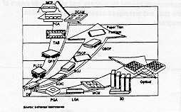 |
packaging trends |
Testability challenges can
be classified as follows:
Design and Test Technology
Gap -- Automatic
Test Equipment (ATE) basically exists to detect and diagnose faults.
ATE must function within an economic balance between the cost
of quality conformance and the cost of non-conformance.
Commercial ATE often provides
high fault coverage test programs, automatically, over the vast
majority of typical designs. However, the design engineer alone
knows which part of the design (usually less than 10%) stretches
the design envelope and requires special test considerations.
Testability can be as simple as alerting the test engineer to
this situation.
Because a tester must provide
a wide degree of flexibility in determining and identifying the
presence of faults, yet minimize the cost of detecting those faults,
its hardware specifications generally trail those of the technologies
that it is testing. For example, the clock and data rates on
the printed circuit board might be 60-100 MHz while a combinational
tester might have a clock rate to 50 MHz and data rates to 10
MHz.
Based on the principle that
'it isn't how fast you test, it's how you test fast,' GenRad has
pioneered many novel and patented test techniques to provide effective
fault coverage to close the technology gap. These innovative test
solutions include techniques such as Scan Pathfinder™ for
boundary scan-based designs, Analog Functional Test Module (AFTM)
for mixed-signal devices, and Deep Serial Memory for in-line programming
and verification of flash memories, etc.
Similar test techniques are
being developed to provide comprehensive test coverage as logic
levels are reduced... 5 volts to 3.3 volts to 1.8 volts... in
response to demand for lower power consumption or more portable
products. GenRad's digital test subsystems provide test programming
flexibility to manage these emerging device trends.
Design simulators establish
timing increments down to pico seconds and simulate long serial
streams of vectors. A test system, however, has a more finite
timing limitation and utilizes more loop-oriented test flows.
GenRad has codeveloped with Diagonal Systems Ltd. a set of tools,
WAVELink™ to compensate for this fundamental difference.
Design Data Availability
-- More and more
frequently, detailed design data that would not only improve test
coverage but also speed up testing is not ordinarily made available
to the test group by the design group. Most often this is the
result of design and test residing in different departments, divisions,
or buildings -- even different companies.
To increase fault coverage
when basic design data is not available, GenRad has developed
vector-less testing concepts: Opens Xpress™ which enhances
the degree of test coverage for manufacturing-induced faults;
and Xpress Model™, an automated test model development tool,
which supports vector-based test techniques to heighten the confidence
in device functionality.
Test Development Time Availability
-- Intense global
competition has dramatically reduced design-to-market cycle times.
Consequently, the time available to develop comprehensive, high
fault coverage test programs has also been dramatically reduced.
GenRad attacks this testability
challenge on several fronts. Powerful design and test integration
tools, CAT-Link™ and WAVE-Link, automate the transfer of
CAD, CAE, and simulation data from a wide range of design environments
into formats required to drive the test generation process.
The performance of automatic
test generators and the debug tool, TEST XPRESS™, has been
enhanced to deliver lightning fast levels of performance to extremely
high levels of fault coverage. This near real-time test generation
allows most fault coverage to be produced automatically. As a
result, the test engineer has more productive time to concentrate
on tests for the more challenging aspects of the design.
Rooted in GenRad's fundamental
philosophy -- "the difference in software is the difference
in test™" -- advanced test and diagnostic algorithms power
more test coverage per unit of test hardware than is available
from any similar board test system.
Test and Fixture Technology
Gap -- Often viewed
as a separate industry, fixturing technology is seen as either
the limiting factor to providing effective testability or as
the facilitator for implementing new test techniques.
GenRad works closely with
fixturing industry leaders. These critical partnerships bridge
the gap between GenRad's core expertise in electrical test and
diagnostics and the fixturing companies' expertise in mechanical
access. This cooperative effort has pioneered many breakthroughs
in advanced fixture technology ... Short Wire Length fixtures
... Opens Xpress probes... wireless fixtures, etc.
GenRad continues to work with
the fixture experts to solve test problems resulting from the
use of no-clean solder, from other contaminants accumulated on
the fixture probes during volume production, or from the need
to precisely align fine-pitch boards to the test interface.
Physical and Electrical
Testability Access -- The
ability to physically access test points for stimulus, measurement,
or diagnostics has been seriously affected. The test engineer
is challenged not only by fine-pitch geometries, tightened packaging
densities, intra-module connections, and flexible circuit boards,
but also by the un-desirability of tester induced faults from
high-speed circuit loading.
GenRad has created many innovative
test techniques and tools -- Multiple Level Inhibits, Boundary
Scan, NAND Tree, Deep Serial Memory, etc. -- that address these
issues. They all increase test fault coverage, even though the
physical access by the test probes is impaired by the application
of the sophisticated device, packaging and interconnect technologies
to the design of the product under test.
Testability Awareness --
GenRad offers products,
support services, and consultancy aimed at enhancing the awareness
of the technological and economic advantages of testability among
members of the test, design, and management staffs. This includes
both design-for-testability considerations and an understanding
of tester limitations relative to design practices. The following
assessment of the state-of-test technology and test techniques
will help you to better understand testability.
The State of Combinational
Test Technology.
There are basically two approaches
to test -- functional and in-circuit test
Functional Test -- Verifying
the Entire Board.
Functional test is characterized
by the application of input stimuli and measurement of the output
signals on the circuit board. The measured output is compared
against an expected result. Sophisticated diagnostic algorithms
guide an operator through an interactive probing sequence to isolate
the particular source of the fault. Test access is assumed to
be available to support the effectiveness of this testing philosophy.
Functional test is aimed at
verifying the functionality of the entire board. Functional test
systems can be executed effectively at the speed of the design.
Functional test systems offer
the potential of very high fault coverage and high confidence
in the test results. However, functional test is based on two
assumptions: the degree to which simulation technology can be
applied to generating the test program, and the degree to which
diagnostic strategies can be developed in a cost-effective and
timely manner.
In-Circuit Test -- Verifying
the Components and the Assembly Process.
In-circuit test is characterized
by the application of stimuli to and measurement of the signal
nodes on the circuit board. In-circuit test is best described
as testing the functionality of each component on the board, with
the inference that the overall board functionality can be verified
by the fact that each component functions and that it is wired
properly.
In-circuit test generally
does not execute at the speeds of the design, due to the fact
that the physics of back-driving limits the technique's practicality
to a range of between I and 10 MHz test speeds. Test access is
assumed to be available at each node to support the effectiveness
of this testing philosophy.
Combinational Test -- The
Way of Life.
Modern ATE has evolved to
a point where functional test is being used in very limited instances.
This is because the automation of functional test generation
and diagnostic algorithms has not been available at economically
viable prices.
In-circuit test has essentially
moved in two different directions, namely:
Combinational Testability.
In order to design-for-testability,
it is necessary to have a basic understanding of the capability
of the combinational tester to provide test and diagnostics.
This is best accomplished by examining the hardware, software,
and fixturing technologies that support combinational test
Automatic Test Generation
(ATG) has greatly enhanced the acceptance of combinational testing
technology as a viable, cost-effective test approach. The ATG
paradigm requires that information be available describing the
components on the board (test models), their interconnects (circuit
description), and their physical location (assembly).
Automatically capturing design
information into the test generation process speeds test program
development. The lack of the design data, on the other hand, can
severely limit test effectiveness.
ATG algorithms calculate the
effect of the circuit on the ability to stimulate and to measure
the attributes of each component In addition, ATG algorithms have
to recognize the measurement accuracies and timing capabilities
of the combinational tester hardware.
The capability of the tester
to effectively isolate each component to accomplish the highest
fault coverage test requires that analog "guard" and
digital "inhibits and disables" be automatically entered
into the program in order to minimize test development time.
The principal limitation to
automatic test generation involves the lack of design data to
create a test model for the devices on the board and to develop
accurate fault coverage.
Mechanical Design Considerations.
PCB test access is typically
accomplished through a bed-of-nails fixture, although new, higher
performance short-wire fixtures are being used more frequently.
On automated manufacturing production lines where boards arrive
at the ATE via conveyors, mechanically actuated fixtures are used.
Because these mechanical fixtures necessitate higher probe reliability,
they require special consideration.
Vacuum Fixtures
Vacuum fixtures require a
free area of at least 0.125" around the perimeter of the
PCB to ensure a good vacuum seal. Mechanical board handlers may
need as much as 0.138" clearance for conveyor rails. Tool
pin flex can be minimized by using at least 0.12" diameter
pins. Sealing integrity can be improved by allowing a clearance
of 0.125" around the tooling pin. Mechanical fixtures require
a clearance of 0.375" for self-registering tapered tooling
pins.
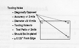
Tooling Holes
Place two (or three) diagonally
opposed, unplated tooling holes as far apart as possible with
a tolerance between holes of ±0.002" to ensure correct
fixture placement. Tooling hole diameters should be maintained
to within 0.003"/-0.000". Solder contamination and plating
thickness variation problems can be prevented by keeping tooling
holes free of plating.
The tolerance from a test pad to tooling hole should also be held to ±0.002". Locate tooling holes at least 0.125" from the board edge to avoid impacting the integrity of the vacuum seal or seating gasket.
 |
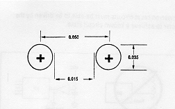
Test Pads
Clear access to test nodes
is vital. Poor access slows production testing and increases
product cost. Ideally, test pads should be provided on each node.
Always place test pads on the bottom of the board to minimize
the likelihood of more expensive double-sided fixtures. Test
pads should be square, if possible, and no smaller than 0.035"
in diameter with pad-to-pad accuracy of ±0.003".
Test pads should also be located
at least 0.125" from the board edge to avoid impacting the
integrity of the vacuum seal or seating gasket. In addition,
pick and place systems and handlers require access to the board
edges.
Test pad spacing should be
ideally 0.100", although some manufacturers implement guidelines
at 0.050" with a minimum of 0.015" separation between
pads.
Test pads on the component
side of the board must have at least 0.040' clearance from components to avoid
damage to either the probe or the part.
Provide an even distribution
of test points to balance the stress from the probe on the board
or the platen. Place them as close as possible to the signal
source to minimize the electrical impact of the tester on the
circuit board. Place several test pads on the VCC and ground
lines to assure a more even power distribution. Keep in mind
that heavy backdrive currents can shift ground potentials.
Accessibility Guidelines for SMT Boards
| 1. Select the largest probe possible. | Larger probes are easier to handle and less prone to damage during handling. |
| 2. Use SMD probes with test centers of 0.050 in. | The SMD probe is designed specifically for SMT boards. Its greater precision ensures probe-tip-target repeatability. Test centers should be 0.100 inches if possible. |
| 3. Use low spring force in densely populated areas. | While higher spring force penetrates contaminants better, a lower spring force used in densely populated areas of your vacuum fixture will ensure proper actuation. |
| 4. Select the proper style for your application. | Some tips will mar or damage circuitry, which may not be acceptable. |
| 5. Test pads should be 0.035 to 0.040 inches in diameter. | Based on generally accepted test fixture/PCB manufacturing tolerances, the SMD probe requires a test pad of this size for repeated tip-to-target accuracy. Naturally, the larger the target, the greater probability of hitting it |
| 6. Coat test pads with conducive non-oxidizing material. | Test pads should be solder coated or coated with a non-oxidizing material such as gold. Solder oxides are easily penetrated with most sharp tip styles, ensuring good electrical integrity. |
| 7. Probe test pads or vias, not components or component leads. | Probing a component lead may make a cold solder joint appear good. |
| 8. Provide accurate tooling pins. | The tooling pin location is key to fixture/PCB alignment Tolerance from the DUT to the datum to the test pad should be ±0.002 in. |
| 9. Place tooling holes as far apart as possible. | Tooling holes on the PCB should be as far apart as possible, diagonally placed, with a tolerance between holes of ±0.002 in. A 0.125 in. or larger tooling pin will help maintain stability and PCB/fixture alignment. Tooling hole diameter should be +0.003/ -0.000 in. |
| 10. Minimize use of tall components. | SMT boards with component height greater than 0.255 in. are difficult to probe, requiring cutouts or relief in the probe plate. When possible, extend test pads 0.2 in. away from tall components to allow for milling tolerances. |
| 11. Don't locate components or test pads too close to the PCB edge. | Location close to PCB edge may interfere with fixture actuation and affect probe-to-target contact. |
| 12. Don't crowd test pads. | Leave a 0.018 in. unpopulated annulus around each test pad to minimize shorting during worst-case tolerance scenarios. |
 |
Positioning and Size |
Probing
Device pins (through-hole),
test pads, connectors, and vias can be used to allow adequate
test access. For PCBs using Surface Mount Technology (SMT), test
pads must be used since probing may damage the leads and open
solder connections may be temporarily disrupted when the probe
moves the leads onto the solder surface.
Ideally, all test access should
occur on the secondary (bottom or solder) side of the PCB. Test
pad diameters must be at least 0.035" when using standard
100-mil (or 75-mil) test probes and should have an adequate solder
surface to ensure reliable probe contact. 50-mil and 75-mil probes
provide less probing accuracy because they allow more flex, in
addition to being more fragile, more expensive, and less reliable.
During test fixture layout, every attempt should be made to minimize
the need for the 50-mil probes. For greater accessibility on
fine-pitch devices, test pads should be staggered to allow 100-mil
spacing.
When probing connectors, probe
density must be carefully planned to avoid conflicts, especially
when vacuum bed-of-nails fixtures are used. Of all test point
access options, vias are the least desirable since they may not
provide the best probing surface.
Where via probing is necessary,
soldering the vias affords a good probing surface and eliminates
the possibility of probe tips catching in unfilled holes. Via
hole filling will also prevent leakage when using vacuum fixtures.
To ensure PCB coplanarity,
increase probing precision, and minimize component damage due
to PCB flexing, test pad density should not exceed 12 per square
inch (8 oz. probes). Excessive probe density may hinder proper
sealing of vacuum fixtures. In every case, probing densities
must be carefully planned to achieve the best testability.
Tall PCB components (>
0.2") necessitate milling the test fixture for extra clearance.
Test pads should not be placed within 0.20" of such components.
As a precaution to avoid damage to the component and to prevent
probe-induced shorts, allow a clearance radius of 0.05".
Electrical Design Considerations.
There are several fundamental
design considerations that can have a major impact on a PCB's
testability and, therefore, its cost.
Power Distribution
While the current handling
capacity of standard probes is 1 amp, a practical limitation of
1/2 amp will guarantee more efficient probe performance and reliable
power distribution. Power distribution should take place across
the entire board with at least three test points for the first
amp and another test point for an additional 1/2 amp. Additional
test points must be included for power supply sense lines, as
well as grounds and returns, especially in digital logic testing.
Any PCB changes, i.e., jumpers or components on the probe surface,
must be positioned carefully so as not to interfere with probe
access.
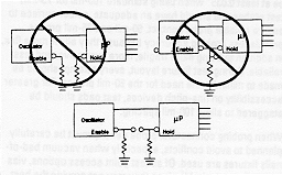
Clocks
On-board clocks must be disabled
to effectively test the rest of the circuit Clock sources must
be controllable from the tester.
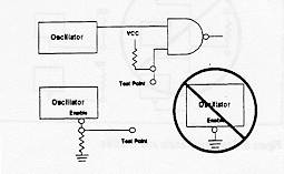 |
Enabling Test
External control or output
lines must not be tied directly to ground or to the VCC. Otherwise,
it's impossible to use available test library elements easily,
leading to a more complex and more costly test routine.
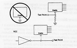 |
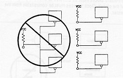
Similarly, separate reset,
control, and enable lines must not be tied through a common resistor
as this prohibits independent testing of each device.
 |
Power-on reset circuits must be able to be driven by the tester to achieve a known circuit state.
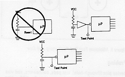 |  |
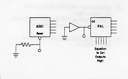
Complex Devices
Make sure that the reset line to an ASIC or the output enable lines on a PAL are accessible to the tester. You may alternatively provide a simple equation that can be entered by the tester to set the outputs of a PAL to a known state.
 |
Frequently, simulation vectors
for ASICs and other custom devices are not available. Automated
test model development tools exist, such as GenRad's Xpress Model,
that quickly develop test models to ensure test activity on each
pin of the device. In conjunction with Hardware Fault Insertion,
these models can quickly be scored for test effectiveness.
Unused Pins
All unused pins must be nailed
with a test pin to ensure that faults associated with these unused
pins do not propagate through the circuit.
Drive Indirect
Many times, lengthy test backdriving of a power device, such as a 244, can lead to device destruction due to excessive heat build-up through the ground pins.
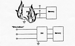 |
Drive indirect is also used to avoid excessive backdrive on a device with a heavy fan-out.
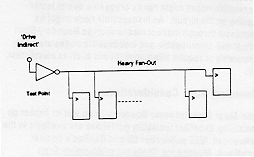 |
Long serial chains also require
special handling to prevent test times from becoming excessive.
Breaking the chain with test access generally slashes the test
time by orders of magnitude.
Flash
Flash EPROMS require special
testability consideration. Do not program the protection bit
until after the test Do not use Hardware Fault Insertion as it
might re-program the device. Program first... then verity.
Battery on Board
An on-board battery requires
a jumper because it is difficult to detect shorts around a battery.
Cluster Test
A bell grid array essentially
has very limited access to its nodes. This often requires a form
of cluster test in which a EGA is tested in conjunction with other
devices that define a more testable functional block.
Mixed Signal Devices
Many analog and mixed signal
devices can react adversely to the electrical loading of tester
and fixture. Test points need to
be buffered or placed
very close to the signal source; alternatively, the device can
be tested as a cluster.
It's there...but can I probe
it?
Circuit nodes fall into two
categories -- those that are accessible or not and those that are
probeable or not. Accessible nodes might not be probeable due
to tester loading on the circuit An inaccessible node might be
probeable through indirect means such as Boundary Scan virtual
nail. Unprobeable and inaccessible nodes are either untestable
or require alternative means such as cluster test, etc.
Boundary Scan Considerations
This paper does not cover
Boundary Scan and its impact on testability. Excellent testability
guidelines are available in the referenced IEEE publication (3)
and GenRad's popular handbook, Meeting the Challenge of
Boundary Scan.
Measuring Testability
Modern ATE provides test facilities
such as Hardware Fault Insertion to automatically grade the effectiveness
of the digital test program. Tools to develop a test figure of
merit for analog circuit are also available.
New Test Approaches
Many innovative testing strategies
are being introduced that will enhance the likelihood of testability.
These include the adoption of Boundary Scan designs, automated
test model development, and analog testing of digital opens.
The Testability Challenge
Regardless of the trends in
system test capability, the basic challenge for test engineers
is not to change the design but rather to make the designer a
believer in testability.
Bibliography
(1) Testability Guidelines
TP-IOIA.
1991 Surface Mount Technology
Association.
(2) Enhancing Test Productivity
and Reducing Test Costs.
1994 Thomas J. Coughlin, GenRad,
Inc.
(3) IEEE Standard 1149.1-1990
(includes IEEE Std.
1149.1a - 1993)
It is also known as 'IEEE
Standard Test Access Port and Boundary Scan Architecture.'
(4) Meeting
the Challenge of Boundary Scan 1994
GenRad, Inc.
Appendix
The ABCs of SMT
Chip carrier
- A low profile surface mount component package (usually square)
with a semiconductor chip cavity or mounting area that is a large
portion of the package size and with external connections on all
four sides. The external connections may be leads or pads.
Component lead
- The solid or stranded wire or formed conductor that extends
from a component and serves as an easily formed mechanical or
electrical connection, or both.
DIP
- Dual in-line package; an IC package with two rows of pins.
Double-sided assembly
- A packaging and interconnecting structure with components mounted
on both the primary and secondary sides.
Fillet
- A smooth, concave junction where two surfaces meet. The quality
of a solder fillet determines the strength of the joint.
Fine-pitch
- <-0.025" spacing of leads.
Flatpack
- An integrated circuit package commonly surface mounted with
gull-wing shaped or flat leads extending from two or four sides
of the package body, with uniform spacing between leads.
Footprint
- The pattern on the PCB to which the leads on a surface mount
component are mated. Also called a land or a Pad.
Gull-wing lead
- A package lead configuration typically used on a small outline
or flatpack package, with a near right angle bend near where the
lead exits the package body and an opposite, 90 bend near the
package base, followed by a 0 to 8 radius bend that forms a heel
and foot An end view of the package with its formed leads resembles
a gull in flight
lnterpackage spacing
- The distance between two or more components on a PCB.
J-lead
- A lead configuration typically used on plastic chip carrier
packages in which leads are rolled underneath the package body.
A side view of the formed lead resembles the shape of the letter
J.
Land
- A portion of a conductive pattern usually used for electrical
connection, component attachment. or both.
Land pattern
- Component mounting sites located on the substrate intended for
the interconnection of a compatible component. Land patterns are
often referred to as lands or pads.
Mixed technology
- A combination of through-hole and surface mount components on
a single PCB.
Pad
- The metal portion of the PCB where the leads on a surface mount
component are mated. Also called a footprint or a land.
Pitch
- The centerline spacing of the leads on an interconnect.
Plastic Leaded Chip Carrier
(PLCC) - A surface
mount package that has 18 to 84 J-leads on four sides with uniform
spacing between leads.
Printed Circuit Board (PCB)
- An epoxy glass and metal composite on which circuits are etched
and to which active, passive, and hardware components are attached.
Reflow soldering
- A process for joining parts by tinning the mating surfaces,
placing them together, heating until the solder fuses, then cooling
in the joined position.
Secondary side
- The side of a package and interconnecting structure that is
opposite the primary side. (it is the same as the solder side
in through-hole technology.)
SIR
- Surface Insulation Resistance.
Small Outline Integrated
Circuit package (SOIC) -
An integrated surface mount package with two parallel rows of
8 to 56 gull-wing leads.
Small Outline J-leaded
package (SOJ) -
An integrated surface mount package with two parallel rows of
J-leads having uniform spacing between leads and rows.
Solder bridging
-The unwanted formation of a conductive path resulting from solder
located between conductors.
Solder fillet
- A normally concave surface of solder at the intersection of
the metal surfaces of the solder connection.
Solder terminal
- A terminal where the electrical connection is made by soldering,
Surface Mount Technology
(SMT) - A method
of packaging and assembling PCBs or hybrid circuits and the components
that are used on them, in which components can be connected electrically
and mechanically to the surface of a conductive pattern.
Type 1
- SMT using surface mounted devices on one or both sides of the
substrate. The assembly is reflow soldered in one or two passes,
depending on the configuration.
Type 2 -
SMT using surface mounted devices on one or both sides of the
substrate and through-hole devices on the component side. The
assembly is reflow soldered on the first pass and wave soldered
on the second pass.
Type 3
- SMT using surface mounted devices on the solder side of the
PCB and through-hole devices on the component side. The assembly
is wave soldered in one pass.
Ultra-fine-pitch
- <0.015" spacing of leads.
Source: G. Derman, ed.,
Connectors and Interconnectors Handbook, Vol.
1, Revised, IICIT, 1990.
The following are trademarks, or registered trademarks, of their respective companies:
Opens Xpress, Scan Pathfinder, Soft Probe, TEST XPRESS, "The difference in software is the difference in test," and Xpress Model - GenRad, Inc.
CAT-Link, WAVE-Link - Diagonal
Systems, Inc.

This Web site was prepared by CciNet's Internet Services